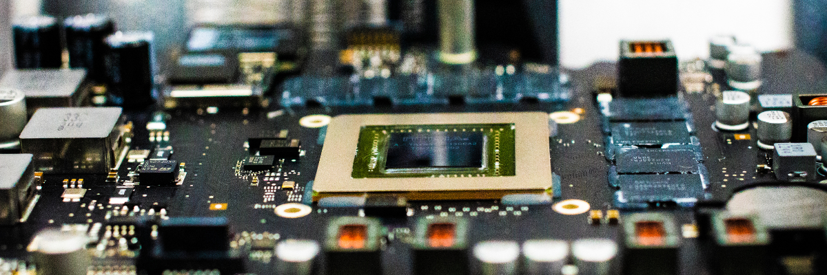
Inspection and testing are crucial steps in the PCB production and assembly process, and are performed at almost every stage. This ensures reliability, performance, and longevity of the assembly and in turn the final product before it’s market launch. However, even the most experienced technicians and manufacturers can make costly mistakes, resulting in defective boards, production delays, increased expenses, and so on. Also, with increasingly complex PCB designs and functionalities, manual inspection is challenging. These errors impact functionality and compromise product safety as well as compliance with industry standards. Understanding the most common testing pitfalls can help streamline production, reduce failures, and improve overall quality. This post highlights common PCB inspection and testing mistakes, and ways to avoid them.
Common PCB Testing Pitfalls and Proven Fixes
Here are common PCB testing mistakes and practical ways to avoid them.
- Skipping the Design for Testability (DFT) Analysis: Many engineers focus on functionality without considering testability, making fault diagnosis difficult and time-consuming. Without proper test access, debugging becomes inefficient and can lead to delays in production. Implementing DFT principles early in the design phase—such as adding accessible test points, boundary scan support, and standardized test interfaces—ensures smooth debugging and allows for automated testing compatibility.
- Ignoring Proper Grounding and Shielding: Improper grounding and inadequate shielding introduce electrical noise, leading to unstable performance, signal interference, and inconsistent test results. Design PCBs with a solid ground plane to minimize these issues, reduce ground loops, and ensure proper isolation between analog and digital sections. Shielding high-frequency components also helps maintain signal integrity and prevents interference during testing.
- Overlooking Power Integrity Issues: Most experts assume that as long as a PCB is powered, it functions correctly. However, power fluctuations, voltage drops, and transient responses can significantly impact performance and stability. To avoid these issues, oscilloscopes, and power analyzers should be used to measure power rails under load, strategically place decoupling capacitors near ICs, and optimize power distribution networks to maintain consistent voltage levels across the board.
- Using Incorrect Test Equipment or Probes: Mismatched test equipment can introduce errors, leading to misleading results. Choosing the right probes for specific signals is essential—for example, active probes for high-speed signals and Kelvin probes for precise resistance measurements. Ensuring proper impedance matching between the probe and circuit also prevents signal distortion and inaccurate readings.
- Failing to Test Under Real-World Conditions: PCBs that pass lab testing may fail in real-world conditions due to temperature changes, humidity, or external interference. To avoid this and ensure long-term reliability, testers must simulate actual environments to test if the boards can withstand temperature fluctuations, humidity, vibration, and electromagnetic interference (EMI). Conducting thermal cycling tests and Highly Accelerated Life Testing (HALT) helps identify potential failure points before deployment.
- Not Performing In-Circuit Testing (ICT): Skipping in-circuit testing (ICT) and relying only on functional testing can neglect component-level defects such as open circuits, short circuits, and incorrect component placements. ICT allows engineers to test individual components before completing functional testing, reducing debugging time and ensuring that manufacturing defects are caught early.
- Neglecting Boundary Scan Testing for Complex Boards: For high-density PCBs with Ball Grid Arrays (BGAs), physical access to test points can be limited, making it difficult to detect hidden defects. Based on IEEE 1149.1 (JTAG) standards, boundary scan testing enables engineers to inspect solder joints and interconnections without requiring direct physical access. This method helps identify issues that traditional inspection techniques might miss.
- Overlooking Signal Integrity Testing: A circuit that works at low speeds does not necessarily function correctly at high speeds. Issues like signal reflections, crosstalk, and timing errors can occur without proper signal integrity analysis. Using tools such as Time-Domain Reflectometry (TDR) and Vector Network Analyzers (VNA) allows engineers to measure signal quality, ensuring proper impedance control and termination.
- Avoiding Visual Inspection: Manual or automated optical inspection (AOI) methods can miss hidden defects such as micro-cracks in solder joints or issues in densely packed BGAs. Relying only on visual inspection increases the risk of undetected failures. X-ray testing provides deeper insight into internal solder joints and component placement, ensuring comprehensive coverage.
- Skipping Final Functional Testing: Some manufacturers assume that passing initial tests is sufficient and proceed with shipping untested boards, leading to catastrophic failures on field. Final functional testing is a must to verify that all power-up sequences, communication protocols, and peripheral interfaces operate correctly before mass production. A comprehensive final test minimizes risks and ensures that the PCB performs as expected in real-world applications.
Avoiding these common mistakes can save money and time while improving product reliability and safety. Integrating rigorous PCB inspection and testing methods makes it possible to enhance PCB quality and performance. If you are still unclear, consulting a reliable player in this segment may benefit in many ways. Rigiflex Technology is one such player, specializing in comprehensive PCB inspection and testing services, which help detect and rectify defects in the manufacturing process, thereby improving the quality and reducing overall costs. They offer custom PCB assembly services. Contact their team of experts for detailed information.
