The continuous technological evolution over the last few decades has led to the development of compact, high-speed, and performance-driven electronic devices. Printed circuit boards serve as the backbone of these devices, and their advancements have enabled increased functionalities, miniaturization, complex circuit layouts, improved signal integrity, optimized power distribution, and more. All of this is essential in today’s fast-paced environment to foster the development of cutting-edge systems and devices. However, if we travel back to the beginning of this digital evolution, printed wiring boards (PWBs) were used to connect essential electronic components. Looking at the rising technological demands today, one may think PWBs must be obsolete by now. But thinking further, one can collaborate with PWBs and PCBs to shape modern electronics, and this post discusses the same.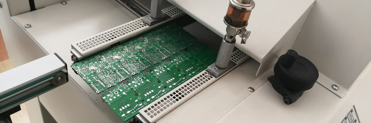
A Brief on PWBs and PCBs
Before getting into their synergy, it is essential to understand these two terms.
- Printed Wiring Boards (PWBs): These boards serve as the main structure in electronic devices, providing a platform for mounting and connecting components. Made from materials like fiberglass or composite substrates, PWBs are etched with conductive copper traces that form electrical pathways. This allows signals to flow between components. PWBs are critical for organizing the layout of circuits and ensuring proper electrical connections within devices. While they focus primarily on physical support and wiring, PWBs enable the design and integration of complex systems, forming the essential base for creating functional printed circuit boards (PCBs) in modern electronics.
- Printed Circuit Boards (PCBs): PCBs integrate the physical structure and electrical pathways necessary for device functionality. Made from materials like fiberglass and composite substrates, copper, aluminum, thermoplastics, and more, PCBs feature etched copper traces that connect various components, facilitating signal transmission and power distribution. They are designed to optimize circuit layouts, ensuring efficient performance, signal integrity, and thermal management. PCBs can vary in complexity, from simple single-layer boards to multi-layer designs used in advanced electronics. Being the backbone of all electronic devices, PCBs ensure that components work together seamlessly, enabling everything from smartphones to medical equipment and beyond to operate effectively.
Synergy Between PWB and PCB
The core relation between PWBs and PCBs is that of foundation and its structure. Together, they can create a functional, interconnected system capable of performing complex tasks. The following pointers help in understanding how their roles intertwine.
- Framework Building: A PWB serves as the structural base of any electronic system. It provides a platform where components are mounted and connected. The PWB is etched with conductive copper traces, which form pathways for electrical signals to travel between components, enabling the system to function as a complete circuit. The primary role of the PWB is to support the physical assembly and ensure signal flow with minimal interference or signal loss.
- Establishing Electrical Conductivity: PCBs take over where the role of PWB ends. Once the PWB structure is in place, the PCB defines the electrical connections between components, ensuring signals flow correctly through the copper traces. The PCB layout optimizes the placement and routing of electrical pathways, enabling components to communicate with each other effectively. Proper PCB design addresses critical factors like signal integrity and power loss, especially in high-speed or high-frequency applications.
- Design Considerations: A successful PWB and PCB integration requires balancing electrical and structural design considerations. Key factors include the thickness of copper traces, their spacing, and the types of components used. Designers must also consider thermal management, signal integrity, and compatibility to ensure the final product performs optimally. Both PWB and PCB designs must work in tandem to meet these critical requirements.
- Manufacturing: The manufacturing begins once the design phase is completed. Initially, the PWB is created as a substrate layer, and copper traces are etched onto the surface to establish electrical pathways. The PCB layout is then incorporated, and components are soldered onto the board. Precision is essential during manufacturing to ensure proper trace width, spacing, and connection points. A poorly executed PWB structure will result in an ineffective PCB design, compromising the final product’s functionality and reliability. Each step must be executed with accuracy to ensure performance standards are met.
- Prototyping, Testing, and Optimization for Production: Once the PWB and PCB designs are complete, testing is the next crucial step. The physical structure and electrical connections must be tested to detect potential faults. Automated optical inspections (AOI) and X-ray scans identify issues like misalignment or defects in the copper traces. Based on these tests, design improvements are made, optimizing the product for large-scale production and ensuring it meets the required functionality, reliability, and durability standards.
At times, PWBs and PCBs may be used interchangeably; however, we now know that they are slightly different in manufacturing methods, materials, complexity, and more. These two can be combined in modern electronics, saving costs and time. Are you an OEM who needs PCB or PWB assembly? In any case, you need to partner with a reliable and experienced PCB assembly service provider. Rigiflex Technology specializes in flexible and custom PCB solutions that exceed the boundaries of modern electronics. Whether you’re working on high-speed circuits, wearable technology, or custom designs, our expertise can help bring your vision to life. Contact us today for further details.
