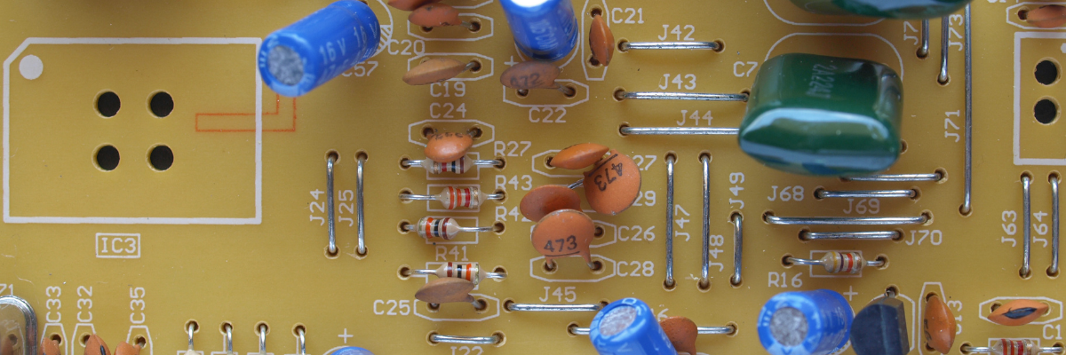
Designing a 10 layer flex circuit board is no mean feat. It requires technical prowess and expertise beyond the grasp of the average Joe. Flexible PCBs have found worldwide acceptance across several industries, domains, and applications due to their functional versatility. However, when assembling PCBs, several issues related to design could occur. These should be avoided to ensure smooth uninterrupted service of the PCB in application.
Assembling PCBs: 3 Common Solder-related Problems
A PCB designer could encounter the following problems:
1. Solder Mask
When the solder mask or cover film is applied on to the PCB, the underlying traces can be affected. The general rules of PCB manufacturing require the manufacturer to take these factors into account. The design and production process should compensate for these shortcomings.
2. Solder Pads
The space between a solder pad and a copper trace should be enough (not more or less) to accommodate the solder mask. If this condition is not satisfied, it could result in shorting.
3. Solder Joints
A solder joint is the joining of solder alloy and copper trace using a solder. This causes the entire space including the trace to become very rigid. Hence, when the PCB is bent, it could cause the alloy to crack. Your manufacturer will be able to join components in a way that the solder joints don’t affect the functionality or flexibility of your PCB.
Keeping a tab on the common problems associated with PCB assembly will also allow you to check the finishing of PCB. This is important to ensure long term efficient functionality of PCBs. By being aware of the common problems, you can conduct an audit. This will give you assurance regarding the quality of work you are receiving from your PCB manufacturer.

