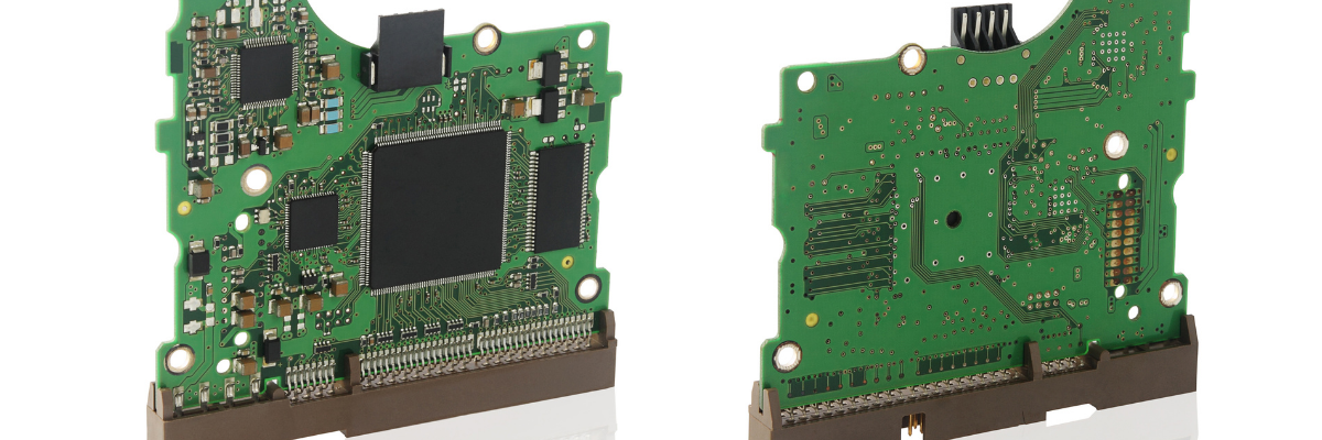
High Density Interconnectors (abbreviated as HDI) is the new age PCB with a higher wiring density than standard PCBs. These boards are characterized by buried/blind vias and microvias .006 diameter, high performance thin materials, and fine lines. Today, these HDI PCBs are used in various industrial applications that demand perfect circuit board operation. This post discusses factors that make HDIs one of the fastest growing PCB technologies.
Brief Introduction to HDI PCB Microvias
The increased wiring density on the HDI PCB allows more functions per unit area. Advanced HDI PCBs feature multiple layers of copper filled stacked microvias that enable complex interconnections. Microvias are minute laser drilled holes on a multilayer circuit board, which allow interconnections between layers. In advanced smartphones and hand-held electronic devices, these microvias cross over multiple layers. Microvias are via-in-pad, staggered, offset, stacked, copper plated over the top, plated, or solid copper filled.
Types of HDI Boards
The HDI Boards are mainly classified into three types:
- HDI PCB (1+N+1): These PCBs feature one “build-up” of high-density interconnection layers. This type of PCB provides excellent stability and mounting. Popular applications include cellphones, MP3 players, UMPC, GPS, PMP, and memory cards.
- HDI PCB (2+N+2): These PCBs have two or more “build-ups” on high-density interconnection layers. Microvias are staggered, or stacked on different layers. This PCB has thin board capabilities. The lower Dk/Df material allows for better signal performance. Popular applications include Personal Digital Assistant (PDA), cellphones, portable game consoles, camcorders, and Differential Scanning Calorimeter (DSC).
- ELIC (Every Layer Interconnection): These PCBs have all high-density interconnection layers, which allow conductors to be freely interconnected with copper filled stacked microvias. These PCBs exhibit excellent electrical characteristics. Popular applications include GPU chips, CPU, memory cards, etc.
Advantages of HDI Boards
HDI PCBs are considered perfect alternatives to sequentially laminated boards, or high layer expensive standard laminates. The following advantages account for their popularity.
- High speed
- High frequency
- Lightweight circuits
- Small size circuits
- No mechanical shocks
HDI boards are currently used for consumer and handheld electronics. They are also being considered for large board designs, and their demand will grow in the future. For more information about HDI – High Density Interconnect PCBs, please visit http://www.rigiflex.com/ or contact the company at (714) 688-1500.

