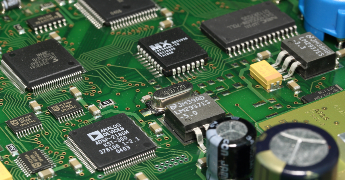
Radio frequency (RF) and microwave circuit boards are significant in mission-critical applications. This is because of their ability to carry signals with varied and especially higher frequencies compared to standard PCBs. Designing these PCBs is expensive and complex; therefore, only military and aerospace industries used them earlier. However, they are now used in wireless networks, smartphones, satellite broadcasters, and other handheld wireless devices, underscoring their versatility. Although the functionality of RF and microwave PCBs is top-notch, it is challenging to design these PCBs and their assemblies considering the frequency variation and complex application requirements. PCB assembly service providers must follow standards and design guidelines while manufacturing RF and microwave PCBs. OEMs must also consider these aspects when sharing requirements or design files with PCB assemblers. This post focuses on the essential design aspects to consider when designing and assembling RF and microwave PCBs.
Key Design Guidelines for RF and Microwave PCB Assembly
Understanding the differences between RF and microwave signals is essential for efficiently designing RF and microwave PCBs. RF signals cover wider frequency ranges, while microwave frequencies range from above 1GHz to about 30GHz. The frequency ranges affect how the signals are managed and the specific design practices needed. Here are some important considerations when designing these PCBs.
- Component Placement: Most of these PCBs have multiple components including a few sensitive ones. Proper component placement is crucial in RF and microwave PCB designs to minimize interference and ensure efficient performance and prevent signal losses. By strategically separating components based on their type, designers can reduce the risk of interference, such as crosstalk, which often occurs when signals of different types are placed in close proximity. This method helps during the assembly process by simplifying layout complexity and enhancing the overall reliability of the circuit. Thus, keeping RF, analog, and digital components grouped separately is a fundamental best practice to avoid unwanted interactions and achieve optimal signal integrity.
- Laminate Materials: The properties of laminate materials directly impact the board’s ability to manage high-frequency signals. Factors such as heat dissipation and dielectric constant determine the board’s efficiency in handling signal integrity and thermal stability. FR4 is a commonly used and cost-effective laminate. However, its performance in high-frequency applications is limited due to its relatively low dissipation factor, leading to signal loss. To ensure better signal integrity, select laminates with high dissipation rates, which provide superior thermal management and minimize signal degradation.
- Stack-up Optimization: The optimization of layer stack-up plays a significant role in the effective design of RF and microwave PCBs. Using multiple layers allows for better organization of signals and components, reducing interference. By assigning specific layers for different functions—such as placing RF signals on the top and reserving others for power or ground—it is possible to isolate sensitive signals, thereby preventing electromagnetic interference (EMI). Lower layers can manage microwave signals, allowing an interference-free layout. As a best practice, a minimum four-layer configuration is recommended to provide adequate separation between different signal types and components, enhancing PCB performance and minimizing potential signal issues.
- Minimizing EMI and Noise: Minimizing noise and electromagnetic interference is another critical aspect while designing these PCBs. This is especially true when dealing with high-density layouts. When traces are placed too close to each other, crosstalk becomes a significant issue. This can lead to signal degradation. To mitigate these effects, increasing the spacing between signal traces is essential to limit the possibility of unwanted coupling. Additionally, proper dielectric spacing helps improve isolation between signals, reducing interference. Implementing shielding techniques, such as using grounded planes between sensitive traces, further minimizes EMI by creating practical barriers against interference. Increasing the spacing between components and employing ground planes are fundamental strategies for maintaining signal clarity and reducing noise in RF and microwave PCB designs. The use of PCB EMI shields or cans also helps suppress internal EMI and acts as a barrier to external EMI signals.
- Impedance Tolerance Management: Slight impedance mismatches can lead to signal reflection and loss at higher frequencies. These issues can degrade the performance of the board. To mitigate these problems, minimizing the length of parallel traces is essential as longer parallel runs tend to create impedance irregularities. By keeping these parallel traces short, designers can maintain impedance levels, ensuring better signal integrity and minimizing losses.
- Reducing Return Signal Loss: This is vital for the reliability of high-frequency RF and microwave PCBs as improper signal paths can lead to signal degradation. An efficient return path is critical in designing these PCBs as it involves optimizing the layout of the ground plane, which acts as the primary path for returning signals. A well-placed ground plane minimizes disruptions and maintains signal quality throughout the board. Consistent ground plane design is essential for improving signal integrity in high-frequency PCB applications.
As an OEM, if you manufacture a product for mission-critical, high-frequency, or any high-heat generating applications, you may want to consider the type of PCB assembly that supports it. Consider inventing in high-quality RF and microwave boards to get the desired output and ensure the overall product quality and safety. For this, you can contact reputed manufacturers like Rigiflex Technology to get the best possible solutions along with custom options to suit your application requirements. The company manufactures and assembles PCBs based on your requirements and has the experience of handling complex requirements. Contact their team today for any further questions you may have about the use of RF and microwave PCBs in your application.

