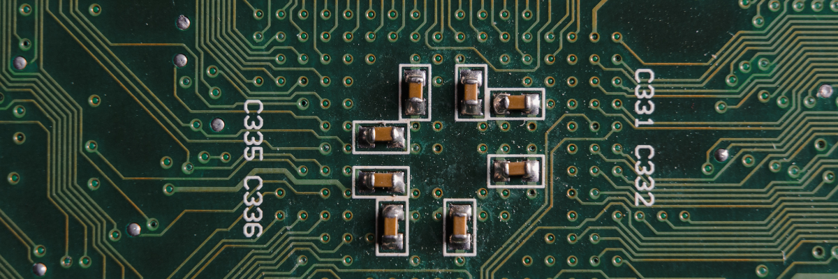
With the size of electronic devices shrinking and their design becoming more and more complex, the demand for small-sized PCBs with maximum components placed accurately has gone up. This has pushed the demand for tools and technologies which facilitate accuracy in such small and complex parts. This is the reason why the High Density Interconnect (HDI) technology has expanded its scope in this segment. This technology enables the construction of extremely dense and small boards, which have a significantly high number of components per square inch effectively mounted on them. This post takes a look at the growth of HDI PCB fabrication and its benefits.
Significance of Using HDI PCB Fabrication
Normally, PCBs have single or two layers. Multilayered PCBs can have anything from three to twenty layers depending upon the application and its complexity. An HDI PCB would have even 40 layers, with accurately mounted components, fine lines, and micro-vias in compact spaces. You can recognize them by their fine lines. HDI PCB fabrication scores on other aspects too. Here are some of them:
- With HDIs, you can have several permutations and combinations of layers.
- Although cores are a part of a PCB layer design and they are shown in the diagram too, HDI enables coreless design.
- You can have two or more HDI layers through vias, and vias through buried vias, and this way have several types of HDI boards.
- The via-in pad process is followed to have maximum components in minimal number of layers.
- If we compare it with the commonly followed through-hole technology, what it achieves in 8 layers is achieved with the help of HDI in 4 layers.
- With HDI, it is easier for the designers to place small components very closely in a compact space.
- HDI PCBs are especially useful in mission-critical applications such defense aircraft and medical devices aside from the regular consumer electronics and automobiles.
Here is a representative diagram of HDI Layering on an 8-Layer PCB:
|
Layer 1 Foil
|
|
Prepreg
|
|
Layer 2
|
|
Core
|
|
Layer 3
|
|
Prepreg (Copper fill) (Laminating material fill)
|
|
Layer 4 (Laminating material fill)
|
|
Core (Laminating material fill)
|
|
Layer 5 (Laminating material fill)
|
|
Prepreg (Copper fill) (Laminating material fill)
|
|
Layer 6
|
|
Core (Copper fill)
|
|
Layer 7
|
|
Prepreg (Copper fill)
|
|
Layer 8 Foil (Copper fill)
|
Benefits of HDI Technology
There are a number of benefits HDI offers to the PCBs and in turn to the product at large. Here are a few of them:
- There is no doubt that the HDI technology offers the highest level of accuracy.
- HDI PCBs have a better signal speed and a relatively low signal loss compared to the previous technologies.
- With advanced machining, you can drill holes of the smallest of sizes, and with HDI, you can accurately produce the inner and outer layers in the most compact PCB spaces.
- With HDI, you can have really small cores and very fine drilling.
- You can achieve tight hole tolerance and controlled depth drilling.
- The microvias can be really small of up to 0.005 in diameter.
- HDI PCB fabrication is cost effective in the long run as it reduces the number of layers.
- By and large, it enhances the electrical performance of the device.
If you are looking for assembling HDI PCBs for your industrial application, make sure you approach a known PCB manufacturer who would understand your requirements and customize accordingly. Rigiflex is a known manufacturer of custom flex and rigid-flex PCBs, and have a market presence of over 20 years. The company has been providing HDI PCB fabrication services to its clients across diverse mission-critical industries for a long time.

