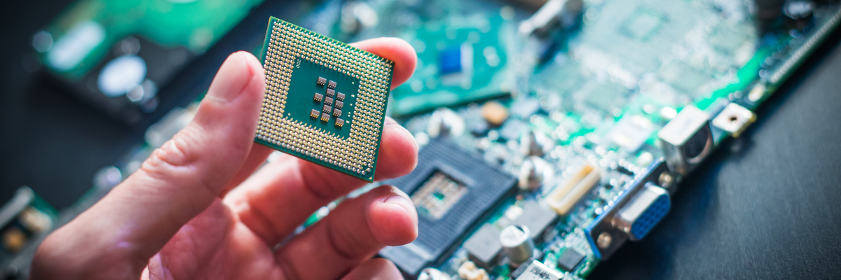
Rigid-flex circuit boards feature both rigid and flexible components, hence the name. These hybrid printed circuit boards are widely used across various industries because they combine the best of both— rigid and flexible circuit boards. Although they have become an integral component of various electronics, their fabrication involves several complex steps. Do you want to know what they are? Read the post to find answers for your questions.
Steps Involved in Rigid-Flex Manufacturing Process
The rigid-flex manufacturing process involves the following steps:
- Base Preparation: How a PCB can be made without a strong base? Thus, the rigid-flex construction starts with a base preparation. The laminate preparation is the first step in the manufacturing process. The laminate features a copper layer, which may or may not have an adhesive coating. Typically the copper sourced from vendors may contain anti-tarnish, which is applied to protect them from oxidation. This anti-tarnish may create problems in the board, thus they are removed by immersing in acid solution.
- Generating Circuit Patterns: How is this done? This can be done in one of the two ways— photo imaging & screen printing. In the first method, the circuit deposits are created directly on the laminate, whereas in the second method, a photoresist film is positioned near the laminate, and exposed to UV rays. These rays help create the pattern on the laminate.
- Circuit Pattern Etching: Etching the circuit pattern is the next step in the process. What does it involve? In this, basically, the circuit pattern generated on copper laminate is etched. This is mainly done by spraying an etchant solution over the circuit pattern or dipping laminate in an etching solution. Etching is performed on both sides of the circuit pattern to achieve the desired results.
- Drilling Holes: This step involves drilling ultra-small to large-sized holes, as well as vias, and pads on the flex substrate. The drilling of holes is performed using lasers. CO2 lasers, as well as infrared or ultraviolet lasers are used for the purpose. This type of laser drilling helps assure precision and minimizes waste.
- Through-hole Plating: It is one of the important steps in the PCB manufacturing process, which demands great precision. Copper is deposited into drilled holes and plated with a chemical. The thickness of through-hole plating is usually maintained at 1Mil. Through-hole plating is performed to create electrical interconnections on the circuit board.
- Coating Etch-Resist: In this step, conducted after the through-hole plating, a photosensitive etch-resist coating is applied on the flexible substrate. There are several etch-resist coating materials in use, of which liquid photo imageable (LPI) is the most popular. Etch-resist can be applied in many ways including spray coating, roller coating, and curtain coating.
- Stripping Etch-Resist: The chemical resist applied to the plated through-hole is stripped in the next step.
- Application of Covercoat or Coverlay: A cover lay is applied on both the sides – top and bottom of the PCB to protect it from harsh environmental conditions, solvents, chemicals, and more. There are several cover lay materials available, however, the combination of a laminated polyimide material with adhesive is most preferred by PCB manufacturers. This coverlay material is screen printed onto the surface of the printed circuit board, and exposed to UV for curing. High temperatures or pressures may affect the adhesion process of coverlay material to the substrate. Thus, this process is conducted under controlled pressure and temperature. In some applications, a cover coat is applied on the PCB sides to ensure protection. A cover coat is directly applied to the sides, and it is not a laminated material like a coverlay.
- Cutting the Flex: In this step, the individual flex board is cut from the production panel, and the process is known as cutting or blanking. This step needs to be performed with extreme caution. Although there are several techniques employed for blanking, hydraulic punching is preferred the most. It is because, this method allows for precision cutting of several circuit boards, and its high tooling costs can be compensated in bulk production. Blanking knives are preferred for prototype creation and other small production runs.
- Lamination: In this step, the flexible circuit board is laminated between the rigid sections. The lamination is made using glass and PI.
- Electrical Testing and Verification: As with any PCB manufacturing process, the-rigid flex PCB fabrication ends with electrical testing and verification. The boards are subjected to electrical testing for ensuring circuit performance, continuity isolation, and quality.
All the above-discussed steps guarantee a reliable and performance-driven PCB for your application. The choice of materials and processes may vary across various manufacturers; however, it is important confirm that your choices don’t impair the quality of the circuit boards. Owing to the popularity of rigid-flex PCBs today, it is quite easy to find manufacturers who specialize in their fabrication process. It is important that you get your boards fabricated from experienced players such as Rigiflex. The company specializes in a single-layer, double-layer, and multi-layer rigid-flex PCBs.

