When it comes to high-speed PCB Design, signal integrity plays a crucial role in achieving reliable and efficient performance. Signal integrity means the preservation of quality and reliability of the electrical signals as they travel through the circuit so that they are free from distortion and work properly. However, several factors can influence signal integrity like via design, ground plane strategies and design for manufacturability (DFM). This post discusses these factors and offers strategies to help PCB designers optimize their designs for superior signal integrity.
Understanding Vias and their Influence on Signal Integrity
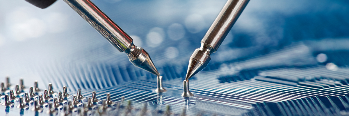
Vias help establish electrical connections between different layers of a multilayer board. There are various types of vias, like through-hole vias, blind vias, and buried vias. Each of these vias serve certain purposes. However, they can also significantly impact signal integrity if not designed correctly.
- Impact of Via Inductance: Vias add unwanted inductance, which becomes problematic at high frequencies. This inductance can cause signal reflections, overshoot, or ringing, which distorts data, reducing the quality and reliability of signals.
- Impact of Via Capacitance: Vias also introduce capacitance, leading to impedance mismatches. Impedance mismatches caused by vias can result in signal distortion and degradation, impacting data accuracy.
How to Optimize Vias for Signal Integrity? Strategies Explained
In order minimize the adverse effects of vias on signal integrity, here are some optimization strategies that designers can employ.
- Place vias symmetrically and close to the ground planes to minimize inductance and capacitance.
- Reduce the number of vias on high-speed signal paths to minimize parasitic effects.
- Remove via stubs or keep them as short as possible to reduce signal reflections.
- Use Microvias as they have minimum parasitic inductance and capacitance compared to traditional through-hole vias.
Ground Plane Strategies for High-Speed PCB Design
Ground planes have a crucial impact on maintaining signal integrity in high-speed PCBs. They offer a return path for signals that reduces electromagnetic interference (EMI) and ensures constant signal performance. A well-designed ground plane can greatly enhance the complete performance of the PCB. Here are some effective techniques for ground plane design:
- Minimize the number of vias on high-speed signal paths to reduce parasitic effects.
- Use multiple ground planes in multilayer PCBs to mitigate ground bounce and enhance the signal integrity performance.
- Do not segment the ground plane unnecessarily, as this can create impedance discontinuities and signal reflections.
Impact of Design for Manufacturability (DFM) in Signal Integrity
Design for manufacturability (DFM) is an essential aspect of PCB design that ensures how the board can be produced efficiently and cost-effectively while maintaining signal integrity. Here are three main DFM considerations specific to high-speed PCBs
- Collaboration with manufacturers: It’s important to work closely with PCB manufacturers from the beginning of a high-speed PCB design project. This collaboration helps ensure that the design meets the manufacturer’s capabilities and limitations, which can prevent costly redesigns and production delays. Here’s why it is essential:
-
- Manufacturers can offer insights into what is feasible according to the equipment and processes. This helps in aligning the design with practical manufacturing capabilities.
- Designers can understand manufacturing constraints and capabilities early to make informed decisions to optimize costs.
- Manufacturers can offer feedback on design choices that might impact the reliability and performance of the PCB, ensuring that the end product meets quality standards.
- Close collaboration allows for quicker iterations during prototyping and testing phases. Manufacturers can provide immediate feedback on prototype builds, enabling faster design refinements.
- Manufacturers can ensure that the design complies with industry standards and regulations, which is crucial for product certification and market acceptance.
-
- Aspect Vias Ratio: The aspect vias ratio is via’s length ratio to its diameter. This ratio is important to ensure the manufacturability and reliability of the vias, particularly in high-speed designs where vias must maintain low parasitic inductance and capacitance.
Here’s why it is essential:
-
-
- High aspect ratios can be difficult to manufacture reliably, which can cause potential defects like incomplete plating or voids.
- The aspect ratio of vias reduce parasitic effects, which can otherwise introduce signal integrity problems like crosswalk and reflections.
-
Now how to implement this:
-
-
- Utilize micro vias or buried vias where high aspect ratios are inevitable. Microvias have lower parasitic effects and are easier to manufacture at small scales.
- Via aspect ratio should be kept based on the manufacturer’s capabilities. So keep it around 10:1 or less. For example, if a via depth is 1mm, then its diameter should be at least 0.1mm.
-
- Stack-up design: Stack-up design means proper arrangement of different PCB layers including signal layers, power, and ground planes. Optimizing stack-up is important to support high-speed signals and minimize crosstalk between traces. Here’s why it is essential:
-
-
- A well-designed stack-up ensures that signal traces have suitable reference planes. It reduces signal loss and maintains the signal integrity.
- Proper stack-up design can effectively isolate signal layers that minimize electromagnetic interference (EMI) and crosstalk along adjacent signal traces.
-
Here’s how to implement it:
-
- Keep signal layers adjacent to power planes to give a stable return path for high-speed signals.
- Utilize multiple ground planes in the stack-up to minimize ground bounce and give powerful EMI shielding.
- Create a symmetrical stack-up design to save it from warping during manufacturing.
Maintaining signal integrity in high-speed PCB design requires an integrated approach that addresses via design, ground plane strategies, and DFM. By comprehending the influence of each component and implementing best practices, designers can create dedicated and high-performance PCBs that fulfil the demands of modern electronic applications. If you are looking for high-quality PCB design with optimized signal integrity, Rigiflex Technologies, Inc. is your one-stop solution.
