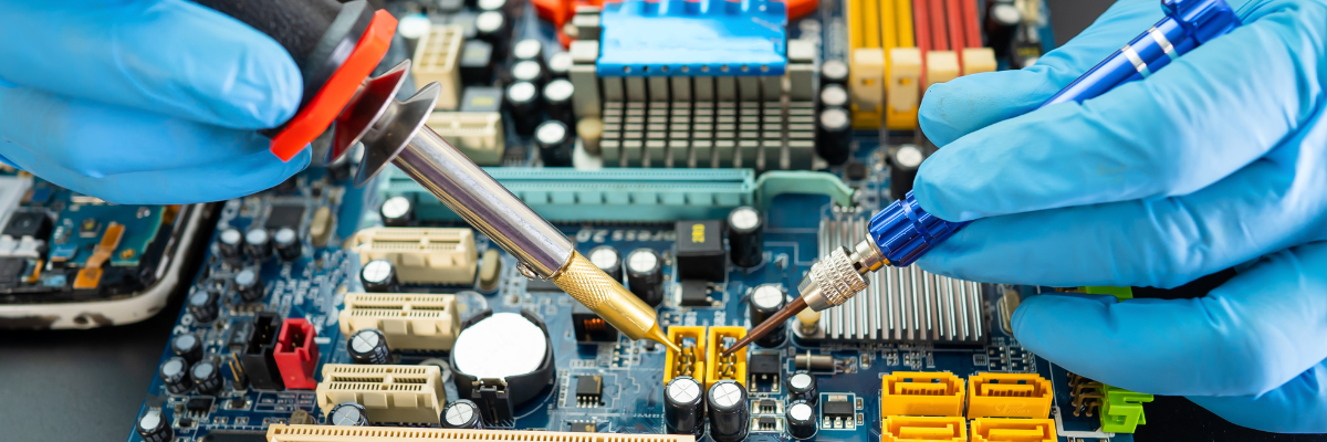
Soldering is a crucial process in electronics that involves joining components to a printed circuit board (PCB) using a fusible metal alloy called solder. This method ensures electrical connectivity and mechanical support for the components, contributing to a reliable and efficient electronic circuit. A solder mask, or solder resist, is a critical layer applied to the PCB to prevent solder bridges between closely spaced solder pads and tracks, thus avoiding short circuits. It not only protects the conductive paths from oxidation and environmental damage but also enhances the board’s durability and performance. The solder mask is typically a green, blue, or black epoxy liquid or dry film that is precisely patterned to expose only the necessary areas for soldering. Its main importance lies in improving the PCB’s reliability, facilitating automated assembly processes, and maintaining the overall integrity and functionality of electronic devices. This blog explores how applying solder mask is crucial for durability and high-quality performance in PCB manufacturing. It also highlights how to choose the right solder mask to maintain excellent quality and reliability in PCB production.
Why Solder Mask is Essential for Reliable PCB Manufacturing?
The application of solder mask offers protection against physical and environmental factors that improves solderability, and facilitates efficient manufacturing and assembly processes. Without a proper solder mask, achieving high-quality, reliable PCBs would be challenging. Below are some of the main reasons why applying solder mask is important.
- Prevents Solder Bridges: Solder mask prevents the solder from bridging between closely spaced pads, crucial for high-density and fine-pitch components.
- Reduces Oxidation: It protects copper traces from oxidation and corrosion, ensuring long-term reliability and performance of the PCB.
- Offers Electrical Insulation: Solder mask provides an insulating layer over copper traces, preventing short circuits and maintaining electrical pathway integrity.
- Improves Solderability: By defining solder areas, it enhances solderability, resulting in clean, precise solder joints critical for reliable PCB assembly.
- Enhances Aesthetic Appeal: Solder mask gives PCBs a professional appearance and can be used for aesthetic purposes or to differentiate between boards.
- Offers Mechanical Protection: It adds a protective layer to the PCB, shielding it from physical damage, scratches, and handling during assembling.
- Facilitates Testing and Inspection: Defined solder mask openings aid in PCB testing and inspection, making quality control processes more efficient and effective.
- Prevents Solder Splashing: The solder mask prevents the solder from splashing onto unintended areas during the soldering processes, thus maintaining circuit design integrity.
How is Solder Mask Applied?
The application of a solder mask is a crucial step in PCB manufacturing, ensuring the reliability and longevity of electronic circuits. The process involves several meticulous steps to achieve a precise and durable coating. Here’s how solder mask is applied.
- Cleaning the PCB Surface: The PCB is thoroughly cleaned to remove any contaminants, ensuring the solder mask adheres properly. This step involves chemical cleaning and rinsing to prepare the surface.
- Applying the Solder Mask Layer: Solder mask is typically applied using a liquid photo-imageable (LPI) process. The liquid solder mask is evenly coated over the entire surface of the PCB, including the copper traces and pads.
- Pre-Drying: After application, the PCB is pre-dried in an oven to evaporate the solvent in the solder mask, making it tacky and ready for exposure.
- Exposure to UV Light: A photomask is placed over the PCB, and UV light is used to expose the areas where the solder mask should remain. The unexposed areas are washed away later.
- Developing the Solder Mask: The PCB is then developed in a chemical solution that washes away the unexposed solder mask, leaving the desired areas covered.
- Final Curing: The PCB undergoes a final curing process, typically in an oven, to harden the solder mask and ensure it adheres permanently to the surface.
- Inspection and Quality Control: The PCB is inspected to ensure the solder mask is correctly applied, with no defects or misalignments. This step may involve visual inspection and automated optical inspection (AOI).
Choosing the Right Solder Mask for PCB Production
Selecting the right solder mask for PCB manufacturing is essential to ensure the quality and reliability of the final product. Below are some of the main key considerations.
- Material Compatibility: Ensure the solder mask material is compatible with the PCB substrate and other materials to avoid adhesion issues and ensure long-term reliability.
- Thermal Resistance: Choose a solder mask that can withstand the thermal cycles of your assembly process, especially if the PCB will operate in high-temperature environments.
- Chemical Resistance: Select a solder mask with good chemical resistance to protect against potential exposure to solvents, fluxes, and other chemicals during assembling and operation.
- Thickness and Coverage: Determine the appropriate thickness and coverage of the solder mask to provide adequate protection without interfering with the board’s functionality, particularly in high-density designs.
- Color and Visibility: Handpick a color that enhances visibility for inspection and testing, while also considering any specific industry standards or aesthetic preferences.
Are you looking for high-quality PCBs with reliable solder mask application to ensure optimal performance and durability? Rigiflex Technology, Inc. offers PCB manufacturing and assembly services that includes precise solder mask application to improve solderability, provide electrical insulation, and protect against oxidation and mechanical damages. We offer custom PCB assemblies. Feel free to contact us today for any queries or requirements.

