This document provides a step by step process of the PCB manufacturing process. The process given below provides information for manufacturing a double sided printed circuit board:
- Collecting Data from the Customer: Data provided by the customer regarding the printed circuit board is taken into consideration. The Gerber files are used to extract the data. Plots and photo plots are developed accordingly.
- Creating an Output File: A PCB software (e.g. CadSoft, Eagle, and Freeware) is used standardize the Gerber data. A processed output file in the format of a Gerber extension is created as a preview of the PCB design. Once the design of the PCB is approved, the other processes of manufacturing begin.
- Material Arrangement: Standard PCB panels are 1.6mm thick, with copper coatings on either side. These panels are cut down to size along with a backup board and the drill entry material.
- PCB Drilling: Two activities take place at this stage. First, all tooling, and reference holes are drilled into the panels. A CNC drilling machine is used to produce component and through hole plated drills.
- Through Hole Plating: An electrographic film is plated to the drill cavity wall. This will support ensuing stages, which will require the copper to be galvanized.
- Resist Lamination, Exposure, and Development: There are three steps in this stage:
- First, the PCB panel is laminated with dry resist film using high temperature and pressure.
- The resist is then exposed to ultra violet rays by using the photo plots.
- The panel is immersed in a solution made from sodium carbonate to develop the panel. Once this has been completed, the electroplating process can begin.
- Electroplating: The PCB’s pads and tracks are electroplated with copper, along with tin film. The film acts as a protective coating, and protects the components during the etching process.
- Resist Stripping: A corrosive solution is used to strip away the photoresist. This is performed to support the forthcoming immersion and spray coat processes.
- Etching: The etching process consists of two stages:
- An ammonia solution coat is sprayed over the copper film to remove any excess material. The galvanized tin protects the components.
- The board is placed in a rinse tank for a few seconds, removed, and then dried.
- Tin Film Removal: Only when the etching process has been completed can the protective tin film be removed. This is performed by using an acid based tin stripper like nitric acid. The tin stripper phase supports PCB spraying processes.
- Soldermask: The soldermask stage consists of three processes:
- Application: There are two ways the soldermask can be applied – either as a liquid varnish, or as a dry film. The soldermask is applied using a hanging casting implement. Once this has been completed, the spraying and screen printing processes can take place.
- Exposure: Like the resist, the soldermask is also exposed to light using the photo plots.
- Development: The PCB is then dipped in a sodium solution. This ensures that any excess soldermask is removed from the pads and soldering points.
- Silkscreen Printing: Once the soldermask processes have been completed, a silk screen is immediately printed on the mask. This process is performed using a legend printer. The printer applies the screen print directly onto the PCB.
- Soldermask Tempering: The PCB is placed in an oven at a temperature of 150°C for 60 minutes. This helps temper the soldermask.
- Surface Finishing: For the surface finishing process, an ENIG surface plating is being used here. As a surface finish, ENIG provides benefits of a flat surface, and acts as a stress free coating. ENIG is a combination of chemicals, nickel, and gold. Using vertical baths, the pads are surface coated with ENIG. The nickel surface ensures solderability, while the gold layer protects the nickel.
- PCB Routing: The final stage is that of PCB routing. However, many times, the panel moves during this phase. To prevent this from taking place, the panel is first pinned down onto the routing machine bed. The PCB is routed using a CNC routing machine. The machine consists of a spindle that moves at fast speeds, providing a high feed rate.
Once all these processes have been completed, the PCB is tested and then sent for client delivery. Knowledge of all the stages of PCB manufacturing can help clients make better decisions, and understand the difficulties faced by PCB manufacturers.
| PCB Manufacturing Capabilities |
| Specifications |
Standard Technology |
Advanced Technology |
| Number of Layers |
1- 12 |
14 – 40 |
| Board Material |
FR4
FR406
IS410
Kapton
Shin-Etsu – Epoxy
Adhesive System
Rogers – Epoxy
Adhesive System
Dupont FR – FR Acrylic
Adhesive System
Dupont LF -LF Acrylic
Adhesive System
Adhesiveless Base Materials |
Aluminum Core
Arlon
CEM
Copper Core
FR408
Getek
Nelco 4000
Rogers 3000
Rogers 4000
Rogers 5000
Taconic TLY
Polyimid |
| Minimum Board Thickness |
2 layer – 0.010″
4 layer – 0.020″
6 layer – 0.020″
8 layer – 0.062″
10 layer – 0.062″
12 layer – 0.062″ |
2 layer – 0.005″
4 layer – 0.010″
6 layer – 0.031″
8 layer – 0.040″ |
| Maximum Board Thickness |
2 layer – 0.125″
3-12 layer – 0.200″ |
0.250″ |
| Maximum Board Size |
16″ x 22″
12″ x 21″
22″ x 28″ |
10″ x 16″
16″ x 22″
12″ x 21″
22″ x 28″ |
| Copper Thickness |
0.5 oz -3 oz |
4oz – 6 oz |
| Hole Aspect Ratio |
7: 1 |
15:01 |
| Minimum Hole Size |
0.008″ |
0.006″ |
| Minimum Trace/Space |
0.006″/0.006″ |
0.003″/0.003″ |
| Minimum |
0.010″ |
0.003″ |
| Drill-to-Copper |
|
|
| Minimum Pitch |
1 mm |
0.3 mm |
| Final Finish |
HASL (Solder)
Lead Free Solder
Copper
Gold
Gold Fingers
White Tin
OSP |
HASL
Gold (ENIG/Hard/Soft)
Selective Gold
Immersion Silver
OSP
White Tin |
| Solder Mask |
LPI:
Green
Black
Red
Blue
Yellow
White
Clear |
LPI:
Green
Black
Red
Blue
Yellow
White
Clear
Mix-and-match
Wet Mask
Dry Film |
| Coverlay |
FR Coverlay
LF Coverlay
Shin-Etsu
Flexible Soldermask |
|
| Silk Screen |
White
Black
Yellow |
White
Black
Yellow
Green
Red
Blue |
| PCB Fabrication |
Scoring
Route & Retain |
Jump Scoring
Route & Retain
Milling |
| Additional Features |
Plated Slots
Non-plated Slots
Controlled Dielectric
Covered Vias
Counter Sinks
Counter Bores
Dual Access Flex
Suspended Leads |
Plated Edges
Plated Milling
Plated Counter Bores & Counter Sinks
Edge Castellation
Controlled Impedance
Silver Filled Vias
Non-Conductive Filled Vias |
| Quality Standards |
IPC 6012 Class 2
Electrical Testing
100% Netlist Testing
TDR Testing |
Milspec 31032
Milspec 55110
Milspec 50884
IPC 6012 Class 3
100% Netlist Testing
TDR Testing |
| Special Technology |
|
Blind & Buried Vias
Laser Drilled Vias
Mechanically Drilled Micro Vias
Metal Core Boards
Burn-in Boards
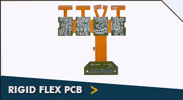
Rigid-Flex Boards
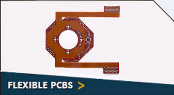
Flex Boards
Micro Circuits |