(714) 688-1500 pcboards@rigiflex.com
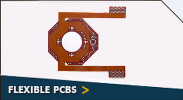
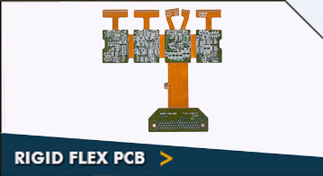
Flex & Rigid-Flex PCBs.. 1-5 Day Quick Turn
Flex & Rigid-Flex PCBs.. 1-5 Day Quick Turn
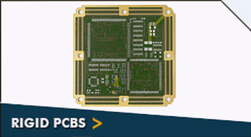
Superior & Trusted Flexible, Rigid-Flex & Rigid PCBs for Over 25 years
HDI (HIGH DENSITY INTERCONNECT PCBS) is one of the fastest growing technologies aimed to increase the functionality of conventional PCBs. Owing to increased, density they provide the necessary routing solutions for large pin-count chips that are utilized in mobile devices and other high tech products.
Features of HDI
There are several key features of HDI PCBs, some of which are as given below:
HDI Builds
HDI PCBs have a much higher wiring and pad connection density than traditional PCBs, due to their design constraint. The structural build up is explained below.
HDI’s Capability
By using HDI technology, designers now have the option to place more components on both sides of a raw PCB. Below are the capabilities of HDIs.
|
Feature
|
Technical Specification
|
|
Number of layers |
4 – 22 layers standard, 30 layers advanced
|
|
Material |
FR4 standard, FR4 high performance, Halogen free FR4, Rogers |
|
Copper weights (finished) |
18μm – 70μm |
|
Minimum track and gap |
0.075mm / 0.075mm |
|
PCB thickness
|
0.40mm – 3.20mm |
|
Maximum dimensions
|
610mm x 450mm; dependent upon laser drilling machine |
|
Surface finishes available
|
OSP, ENIG, Immersion tin, Immersion silver, Electrolytic gold, Gold fingers |
|
Minimum mechanical drill
|
0.15mm |
|
Minimum laser drill
|
0.10mm standard, 0.075mm advanced |
Applications
HDI PCBs are utilized to meet the market demand for complex designs PCB in smaller form factors across the majority of market segments.
This advancement in PCB technology is driven by the miniaturization of components and semiconductor packages that support advanced features in revolutionary new products. The professionals at Rigiflex are always ready to provide you with the best service. For more information, give us a call at 714-688-1500.
All Fields are Mandatory (*)